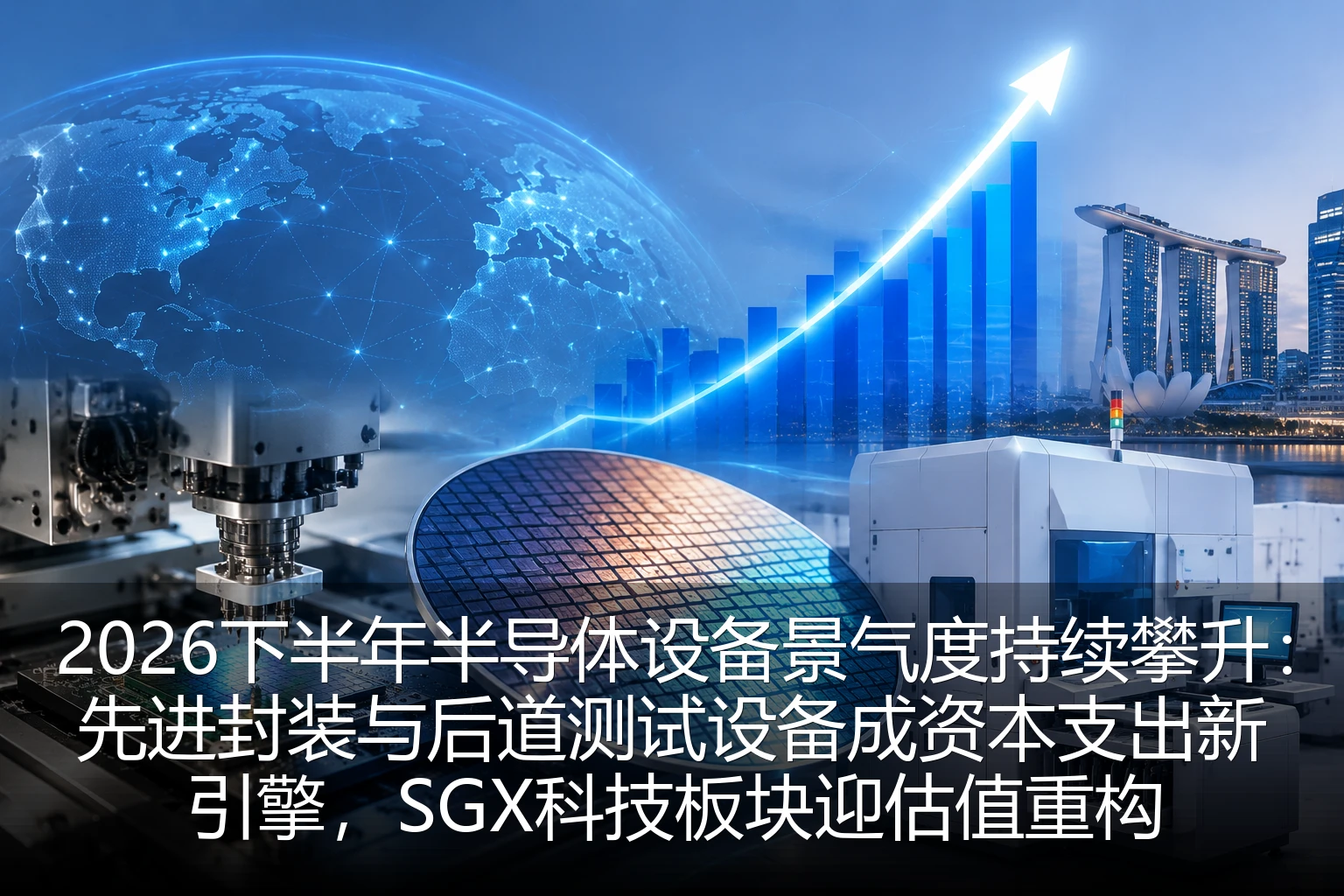
Entering August 2026, the global semiconductor market is undergoing a profound structural reshaping. If the semiconductor market in the past two years was mainly driven by the advanced process competition of front-end wafer foundries and the supply-demand imbalance of storage chips, then the narrative logic of the current second half is undergoing a significant shift - the capital expenditure focus of the semiconductor equipment market is tilting towards back-end advanced packaging and finished product testing equipment at an unprecedented speed. This trend not only marks the paradigm shift of chip manufacturing from "pursuing transistor density" to "pursuing system-level interconnection bandwidth", but also provides a new valuation anchor for global technology investors, especially the semiconductor sector of the Singapore Stock Exchange (SGX).
1. AI computing power evolution reconstructs equipment expenditure logic: from "shrinkage era" to "interconnection density era"
In the second half of 2026, as the parameter scale of large models reaches the trillion level, the marginal cost of improving computing power solely by relying on transistor shrinkage is急剧攀升. Although leading foundries such as TSMC are steadily advancing in 2nm and A16 processes, the industry gradually discovers that the performance improvement of a single chip brought by advanced processes can no longer meet the demand of AI clusters for massive data throughput. At this time, advanced packaging technology that improves interconnection density and bandwidth between chips officially takes over as the core to break through the computing power bottleneck.
This technological evolution directly reshapes the procurement logic of semiconductor equipment. Traditionally, the bulk of capital expenditure for wafer fabs has long been occupied by front-end EUV lithography machines and other equipment. However, the latest industry survey data shows that in the 2026 global semiconductor equipment expenditure structure, the proportion of capital expenditure for equipment such as CoWoS, SoIC and other 2.5D/3D packaging technologies is expected to increase significantly. Orders for hybrid bonding equipment, high-precision placement machines and wafer-level packaging lithography equipment are showing explosive growth. Due to the extremely high alignment accuracy requirements of advanced packaging and complex process steps, the equipment capital expenditure required per chip packaging has even approached some mature process nodes in the front-end.
This change means that the prosperity of equipment manufacturers is no longer solely tied to the iteration of logic processes. Those equipment manufacturers with technical barriers in the field of advanced packaging are ushering in an ultra-long boom cycle far exceeding the industry average. From the macro perspective of the semiconductor market, the prosperity on the equipment side is being transmitted downstream, and the capacity bottleneck of high-density interconnection packaging directly pushes up the packaging quotation of high-end AI chips, thereby reshaping the overall wafer quotation system.
2. Back-end testing equipment welcomes both volume and price increase: complex chip architecture drives up testing demand
In addition to advanced packaging, semiconductor back-end testing equipment has also ushered in structural high prosperity in 2026. As Chiplet architecture becomes the mainstream of AI chip design, a single package integrates multiple bare dies of different process nodes. While this heterogeneous integration improves computing power, it also brings unprecedented testing challenges.
First, the Chiplet architecture causes a sharp increase in chip pin density, and the demand for high-frequency signal test channels is multiplied. Traditional automatic test equipment (ATE) is gradually overwhelmed in terms of the number of channels and test bandwidth, forcing wafer fabs and packaging and testing factories to upgrade to advanced test machines that support higher data rates. Secondly, 3D packaging makes the thermodynamic characteristics inside the chip more complex, and thermal flow testing and system-level testing must be involved at an earlier stage to reduce the high cost caused by poor packaging.
Therefore, in 2026, the orders for global back-end testing equipment have shown a significant "increase in both volume and price". The demand for high-end SoC testers and memory testers has not slowed down due to the mild recovery of consumer electronics, but has continued to strengthen driven by AI computing power chips. The average selling price of testing equipment is steadily rising, and the increase in testing time cost has also indirectly pushed up the quotation baseline of the overall IC market. For the semiconductor market, the testing link is gradually changing from the previous "cost center" to a "value center" that affects the final yield and delivery cycle of chips.
3. Rise of local supply chain and regional balance: strategic opportunities for SGX technology enterprises
Against the background of the accelerated reconstruction of the global semiconductor supply chain pattern, Singapore, as an important hub for global semiconductor manufacturing and R&D, its industrial cluster effect is increasingly prominent. Many technology and semiconductor equipment-related supply chain companies listed on the Singapore Stock Exchange (SGX) are deeply benefiting from the structural expansion of this round of equipment capital expenditure.
In the past, the global semiconductor equipment market was highly concentrated in a few giants in the United States, Japan and the Netherlands. However, with the trend of increasingly strict export controls on semiconductor equipment by geopolitical policies and the increase in supply chain resilience requirements of wafer fabs, the "localization" and "multi-source" procurement trends in the equipment market have become particularly obvious in 2026. Some local and Southeast Asian equipment suppliers with细分 technical advantages have gradually begun to enter the supply chain system of leading wafer fabs.
In the field of advanced packaging, such as temporary bonding/debonding equipment, plasma cleaning equipment and specific packaging lithography equipment, are becoming new breakthrough directions. In the SGX technology sector, listed companies involving semiconductor materials, precision mechanical parts and specific process equipment are seeing their order visibility extend to 2027. These companies, with their deep accumulation in the细分 market, not only occupy a place in the global equipment market, but also gain excess market share growth under the trend of regional balance in procurement.
From the perspective of investment logic, the valuation model for these companies is undergoing a change. In the past, semiconductor equipment stocks were regarded as traditional manufacturing stocks with strong cyclical attributes. However, with the long-term and rigid demand for advanced packaging and testing equipment, the profit volatility of these companies has been significantly reduced, showing the characteristics of technology growth stocks. Capital is beginning to give these细分 leaders with deterministic growth higher P/E rate premiums.
4. Semiconductor market outlook: equipment prosperity is transmitted to materials and IC quotations
Standing at the time node of August 2026 and looking forward to the next six months of the semiconductor market, the high prosperity of the equipment side will eventually be transmitted to a wider range of industry chain links. First, the expansion of advanced packaging capacity directly drives the demand for high-end substrates, ABF substrates and packaging materials. Since these materials also have extremely high technical barriers and long capacity expansion cycles, it is expected that a supply-demand tension similar to the previous silicon shortage will appear in the packaging material end from the end of 2026 to the beginning of 2027, thereby pushing up material quotations.
Secondly, the structural change in equipment capital expenditure essentially reflects the increase in the comprehensive cost of chip manufacturing. In the context of rigid AI computing power demand and strong willingness to pay, this part of the cost increase will be smoothly transmitted to end customers. We have observed that since the second quarter of 2026, leading foundries have conducted multiple rounds of price increases for chips using advanced packaging processes, with a significant increase higher than ordinary mature processes. This structural price increase is reshaping the overall wafer quotation system, making the semiconductor market show a local overheating feature in advanced processes and packaging while showing a mild recovery as a whole.
For investors and corporate decision-makers, the current market environment requires us to break out of the traditional "silicon cycle" framework. The driving force of the semiconductor market is no longer solely dependent on the recovery of terminal consumption such as smartphones or PCs, but is deeply bound to the long-term process of global AI infrastructure construction. The direction of capital expenditure on the equipment side is the leading indicator of the evolution of the semiconductor market.
Conclusion: grasping the long-term investment mainline in the equipment side change
To sum up, the global semiconductor equipment market in the second half of 2026 is at a key node of technological paradigm transformation. The rise of advanced packaging and back-end testing equipment is not only an engineering solution to cope with the AI computing power bottleneck, but also an economic solution to reshape the value of the global semiconductor industry chain. This trend injects new long-term growth momentum into the semiconductor market.
For the technology and semiconductor sector of the Singapore Stock Exchange (SGX), this is not only the growth of order volume, but also a historic opportunity for the upgrading of industrial status. In the wave of equipment domestic substitution and regional supply chain reconstruction, those listed enterprises that can accurately position the细分 track of advanced packaging and testing equipment and have core R&D capabilities are expected to continue to enjoy valuation premium in the future capital market. Investors should pay close attention to the structural changes in semiconductor equipment capital expenditure and use it as the core wind vane for judging chip price trends and grasping the investment rhythm of the technology sector. In the great era of AI reshaping the global computing power foundation, the long-term investment mainline of the equipment track has become clear.