Introduction: Computing Power Surge Breaks Process Physical Limits, Packaging Becomes the New Battlefield
In the second half of 2026, the global semiconductor industry is undergoing an unprecedented narrative restructuring. For the past sixty years, the core logic of semiconductor investment has always revolved around Moore's Law—investors tracked the nanometer process node arms race among TSMC, Intel, and Samsung to judge the cyclicity and prosperity of the chip industry. However, as the demand for computing power from large AI models grows exponentially, the area of a single chip has approached the physical limit of lithography reticle size, and the economic benefits of advanced process transistor scaling are diminishing sharply. Against this backdrop, system integration technologies centered on Chiplets and 2.5D/3D advanced packaging are rapidly replacing traditional process scaling as the true bottleneck determining global AI computing power supply. The underlying logic of why we invest in chips is undergoing a paradigm shift.
1. Chiplets and Advanced Packaging: A Technological Breakthrough Breaking the Reticle Limit
To understand the structural changes in the current semiconductor supply chain, we must first understand why advanced packaging has become a bottleneck. In chip design, there is a physical upper limit to the chip area exposed in a single lithography step, known as the reticle limit, typically around 858 square millimeters. Driven by the demands of AI training large models, the GPU chip areas of leading vendors like Nvidia have approached or even need to exceed this limit. If monolithic chip design continues to be used, not only will the yield drop exponentially with area, but the cost will also become prohibitively high.
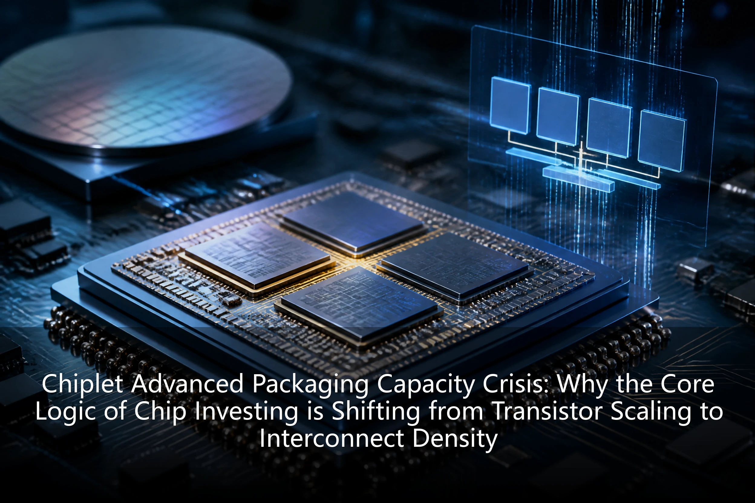
To solve this pain point, the Chiplet architecture emerged. It splits the originally large monolithic chip into multiple small chips, and reassembles them like building blocks on the same substrate through ultra-high-density interconnect and advanced packaging technologies. This architecture not only allows different modules to use different process technologies to optimize costs, but also dramatically improves yield and computing power density.
However, the popularization of Chiplets has shifted the difficulty originally concentrated in front-end wafer manufacturing processes to back-end advanced packaging. Taking TSMC's CoWoS (Chip on Wafer on Substrate) technology as an example, it requires creating ultra-high-density through-silicon vias (TSVs) on a silicon interposer and bonding GPU dies with HBM (High Bandwidth Memory) with ultra-high precision. This process not only requires a large amount of equipment comparable to or even more complex than advanced process nodes, but is also limited by the technical capabilities and capacity of a very small number of packaging fabs. In 2026, with the full-scale explosion of AI inference and training demands, the extreme shortage of advanced packaging capacity has directly choked the global computing power supply chain.
2. The Transmission Chain of the 2026 Capacity Crisis: From Computing Power Hegemony to Supply Chain Restructuring
Entering 2026, the global AI computing power arms race has spread from the large model algorithm layer to the underlying hardware infrastructure layer. Because TSMC's CoWoS capacity expansion speed is far behind the order growth rate of AI chip giants, the entire supply chain shows an obvious structural mismatch. This mismatch has profoundly reshaped global semiconductor supply chain dynamics.
First, the focus of capital expenditure by computing power oligarchs is shifting. In the past, cloud service providers and AI giants primarily directed massive capital toward booking advanced process wafer capacity; now, they have to devote large amounts of resources to securing capacity shares for advanced packaging. Because packaging capacity directly determines how many usable high-performance AI chips can be ultimately delivered, the allocation of advanced packaging substrates and interposers has become a new focal point in the game between chip giants and foundries.
Secondly, the shortage of advanced packaging capacity is triggering a structural reshaping of the price system. TSMC has not only raised foundry quotes for advanced processes but also implemented substantial price increases for packaging services like CoWoS. This cost-side pressure is transmitted down the supply chain and ultimately paid for by end AI customers. Since computing power has an irreplaceable strategic necessity attribute at the current stage, this price hike has not led to demand suppression, but instead triggered deeper panic hoarding, further exacerbating the structural differentiation of market conditions.
Finally, this bottleneck effect is driving a diversified restructuring of the supply chain. To break free from absolute dependence on a single packaging giant, the world's leading chip design companies have begun actively seeking alternative capacities with advanced packaging potential. This has brought a new wave of capacity investment fever to the global semiconductor supply chain and reshaped the valuation system of the wafer foundry market.
3. Rewriting the Logic of Chip Investment: From Process Nodes to Interconnect Density
For investors who have long followed the semiconductor industry, understanding the disruptive significance of this technological change on investment decisions is crucial. Why invest in chips? The standard answer in the past was often: because a certain company has mastered the most advanced process node and can produce transistors with the strongest performance and lowest cost. But in the Chiplet era, this answer must be rewritten: what determines chip performance and cost in the future is no longer just transistor size, but the interconnect density and bandwidth between chips, and between computing units and memory units.
This shift has profoundly affected the investment value of various segments in the semiconductor industry chain:
- The Evolution of Foundry Giants' Moats: TSMC is able to maintain its monopoly in the advanced packaging field not just because it possesses advanced processes, but because it has moved the logic of advanced processes forward into the packaging stage. By utilizing silicon interposers in CoWoS, TSMC essentially accomplishes wafer-level manufacturing during the packaging phase. For investors, evaluating a foundry's core competitiveness must incorporate its advanced packaging capacity into the core valuation model.
- The Leap in IC Design Companies' Architectural Capabilities: In the monolithic chip era, the core competitiveness of chip design companies lay in logical design and IP accumulation. In the Chiplet era, design companies must possess strong advanced packaging architectural capabilities. How to partition modules, how to choose different process nodes for mixing and matching, and how to ensure signal integrity and thermal management during multi-chip co-operation have become new technical barriers. Chip companies with this system-level architecture definition capability will receive a premium far exceeding their peers.
- New Incremental Markets for Semiconductor Equipment and Materials: The equipment demand for advanced packaging is completely different from traditional packaging. It requires the introduction of more front-end process equipment, such as lithography machines, etching machines, and PVD/CVD equipment, used to manufacture high-density micro-vias on substrates and interposers. At the same time, demand for high-end equipment used in wafer bonding and bump manufacturing is also exploding. This brings a brand-new long-term growth curve to the semiconductor equipment sector, and the order fullness of related equipment vendors continues to exceed expectations.
4. Mapping and Investment Strategies for the SGX Tech Sector
Under the grand narrative of global semiconductor supply chain restructuring, the Singapore Exchange (SGX), as an important technology and semiconductor financing center in Asia, is also quietly changing the business layout of its listed tech companies. The SGX tech sector covers numerous precision manufacturing, semiconductor equipment components, and material suppliers located at key nodes of the global semiconductor industry chain.
As advanced packaging becomes an industry bottleneck, tech companies in the Singapore market with relevant technological reserves are ushering in historic development opportunities. For example, SGX-listed companies holding advantages in semiconductor lead frames, high-precision substrates, and packaging thermal management materials are gradually penetrating from traditional packaging into the advanced packaging field, with added value increasing significantly. In addition, Southeast Asia, as a traditional powerhouse for global semiconductor back-end packaging and testing, is benefiting from this wave of advanced packaging capacity expansion, and regional infrastructure and supply chain supporting enterprises are welcoming massive incremental capital expenditures.
For investors laying out the tech sector, current investment strategies need to shift from mere process followers to system-level architecture insighters. When selecting semiconductor concept stocks in the SGX market, focus should be placed on the following dimensions:
- Technological Positioning Advantage: Whether a company possesses an irreplaceable positioning advantage in specific materials, high-precision mechanical components, or specific process steps required for advanced packaging. This technological barrier will directly translate into long-term pricing power.
- Depth of Customer Binding: Advanced packaging demands extremely high supply chain stability. Enterprises that have established joint R&D or deep long-term supply relationships with global top-tier IDM vendors or wafer foundry giants have much higher earnings certainty than traditional general-purpose suppliers.
- Capital Expenditure Conversion Efficiency: Against the backdrop of current advanced packaging capacity shortages, companies able to rapidly expand high-value-added capacity and quickly convert industry prosperity into actual revenue and profit will exhibit extremely strong earnings elasticity in the upcoming earnings season.
5. Conclusion: Packaging Density Determines Computing Power Hegemony for the Next Decade
Looking back at the decades of development in the semiconductor industry, every major technological paradigm shift has spawned new industry giants and also forced participants clinging to old logic to exit the stage quietly. In 2026, we are standing at such a historic turning point. Transistor scaling remains the foundation, but the key to determining computing power limits and commercial success has irreversibly shifted to advanced packaging and system-level interconnects.
Why invest in chips? Because chips are the infrastructure of the AI era and the underlying physical cornerstone of the digital economy. At this specific point in time, the logic of investing in chips has become more three-dimensional and profound: what we are investing in is no longer just the ultimate pursuit of nanometer numbers, but the redefinition of heterogeneous computing architectures and the extreme widening of channels for data to travel at high speeds within silicon. The crisis in advanced packaging capacity is not the end, but the starting point of a new round of semiconductor technological revolution and capital feast. In the wave of global computing power restructuring, only investors who deeply understand this underlying logical change can accurately capture the core assets that truly transcend cycles in the tech investment cycle of the next decade.