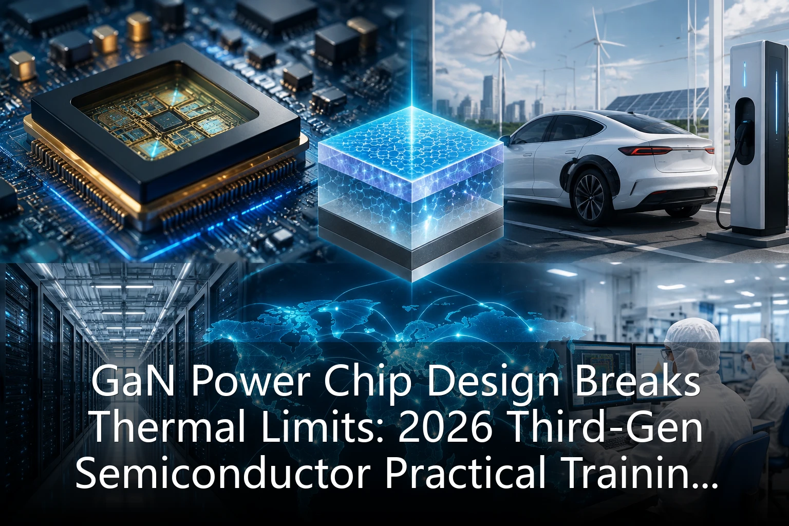
In August 2026, the global semiconductor industry is in a subtle period of technological generational transition. As silicon-based Moore's Law increasingly approaches its physical limits, third-gen wide-bandgap semiconductors, represented by gallium nitride (GaN) and silicon carbide (SiC), are reshaping the global chip supply chain landscape at an unprecedented speed. Especially against the backdrop of the comprehensive popularization of 800V high-voltage platforms for new energy vehicles and AI data center computing power consumption breaking the 100kW per cabinet mark, traditional silicon-based power devices can no longer meet the stringent demands for extremely high power density and conversion efficiency. This makes GaN power chip design the forefront of current semiconductor practical training and technical breakthroughs. However, as power density continues to increase, the thermal limit problem of GaN chips has become the core bottleneck restricting their leap into high-power applications. How to break this thermal limit through substrate technology breakthroughs and packaging process innovations not only tests the practical capabilities of global chip design engineers but also profoundly affects the global semiconductor supply and demand structure and the investment logic of the Singapore Exchange (SGX) tech sector over the next five years.
I. Approaching Thermal Limits: The "Achilles' Heel" of GaN Power Chip Design
As a star material of third-gen wide-bandgap semiconductors, gallium nitride has superior electron mobility, higher breakdown electric field, and lower on-resistance compared to traditional silicon-based materials. Over the past few years, GaN power chips have achieved widespread commercial applications in fast chargers and low-voltage consumer electronics. However, the new industry pain point in 2026 is that when the power density of GaN devices is pushed to several watts per square millimeter, and even expands to kilowatt-level industrial and automotive applications, heat dissipation becomes a fatal "Achilles' heel."
In traditional silicon-based chip design, engineers often solve heat accumulation problems by optimizing circuit topologies or adopting mature heat sinks and liquid cooling systems. However, the high heat flux density generated by GaN devices in extremely small volumes makes traditional thermal management solutions inadequate. The inability to export heat in a timely manner not only leads to decreased electron mobility and device performance degradation but also triggers thermal runaway, severely shortening chip lifespan. From the perspective of semiconductor practical training, current chip design engineers must step away from purely electrical design thinking and shift towards a new paradigm of "thermal-electrical co-design." This requires semiconductor process courses and integrated circuit practical training to be comprehensively upgraded, deeply integrating thermal simulation and packaging thermal resistance analysis into the front-end processes of chip design.
II. Substrate Technology Breakthroughs: The Leap from GaN-on-Si to Bulk GaN
To fundamentally solve the thermal limit problem of GaN chips, the core lies in the underlying innovation of substrate materials. Currently, mainstream GaN power devices on the market mostly use GaN-on-Si epitaxial technology, i.e., growing GaN layers on silicon substrates. Although this solution effectively reduces manufacturing costs and is compatible with existing 8-inch wafer foundry production lines, the huge lattice mismatch and thermal expansion coefficient difference between silicon and GaN limit the thermal conductivity.
In 2026, bulk GaN substrate technology has reached a critical turning point in industrialization. Unlike GaN-on-Si, bulk GaN substrates have unparalleled thermal conductivity (up to 230 W/m·K, far exceeding silicon's 148 W/m·K), capable of rapidly conducting heat generated inside the device to the package shell with extremely low interface thermal resistance. Additionally, by eliminating the stress issues caused by lattice mismatch, the defect density of bulk GaN devices is significantly reduced, allowing them to withstand higher operating voltages and junction temperatures.
This technological breakthrough has had a disruptive impact on the chip design process. In cutting-edge courses at semiconductor practical camps, students no longer merely focus on the conventional PDKs (Process Design Kits) provided by wafer foundries; instead, they need to deeply understand the physical properties of bulk GaN substrates and master device physics modeling and TCAD simulation technologies based on new materials. This vertical integration capability from the material end to the system end is becoming a core metric for measuring an excellent power chip designer and is currently one of the areas with the largest talent shortage in the global semiconductor industry.
III. Advanced Packaging and Thermal Management Reshaping the Semiconductor Supply Chain
In addition to breakthroughs in substrate materials, advanced packaging technology is equally a key starting point for cracking GaN thermal limits. In the 2026 semiconductor industry landscape, advanced packaging is no longer just a means to improve the interconnect density of computing chips; it is also the core path for power semiconductors to break through power density bottlenecks.
1. Double-Sided Heat Dissipation and Copper Clip Interconnect Technology
Traditional wire bonding packaging generates significant parasitic inductance in high-frequency, high-power GaN devices, affecting switching performance and exacerbating high-frequency losses. Currently, a double-sided heat dissipation package architecture based on direct copper clip bonding is becoming the standard configuration for high-power GaN chips. This packaging method not only reduces parasitic inductance by nearly 50% but also achieves dual-channel thermal management that exports heat simultaneously from the top and bottom of the chip. When semiconductor procurement decision-makers evaluate power module suppliers, package thermal resistance has become a core parameter equally important as on-resistance.
2. Wafer-Level Packaging and Leadless Interconnects
To further reduce package size and improve thermal performance, the application ratio of wafer-level packaging in GaN power devices is rapidly climbing. By eliminating traditional lead frames and using photolithography and electroplating processes to directly form redistribution layers and copper pillars at the wafer level, the thermal resistance of GaN chips is further approaching the theoretical limit. This technology trend is reshaping the ecology of the chip supply chain; the boundaries between IDM manufacturers and wafer foundries are increasingly blurring, and the voice of packaging and testing factories in the supply chain is rising with the elevation of thermal management technology barriers.
From the dynamics of the global chip supply chain, foundries with advanced packaging capacity are capturing more GaN order dividends. Meanwhile, the Southeast Asian region, particularly Singapore, as a global semiconductor packaging and testing hub, is leveraging its deep accumulation in advanced packaging to undertake this wave of industrial spillover dividends driven by wide-bandgap semiconductors. Among SGX semiconductor stocks, targets involving advanced packaging and thermal management materials are ushering in continuous revaluations by institutional funds.
IV. Comprehensive Reconstruction of the 2026 Semiconductor Practical Training System
Facing the full-link technological transformation of GaN power chip design from materials, packaging to applications, the traditional semiconductor training system has lagged significantly behind. Currently, the industry urgently needs practical composite talents who can bridge theory, simulation, tape-out, and testing. This has also prompted vocational training and executive seminar programs such as the "Semiconductor Practical Camp" to undergo a comprehensive course reconstruction in 2026.
- From Planar to 3D Thermal-Electrical Co-Simulation: Practical courses are no longer limited to simple SPICE circuit simulations but have introduced thermal-electrical co-simulation practical modules. Students need to learn how to accurately evaluate the thermal distribution and thermal stress of GaN devices under power cycling and short-circuit transients to avoid design failures caused by thermal runaway.
- Mastery of Design Rules Across Process Nodes: With the coexistence of bulk GaN, GaN-on-Si, and even future ultra-wide-bandgap gallium oxide materials, practical training requires students to master the differences in design rules under different substrate materials. Understanding the process capability boundaries of wafer foundries between 8-inch GaN-on-Si production lines and 4-inch bulk GaN production lines has become a prerequisite for successful chip design tape-outs.
- System-Level Application-Oriented Chip Definition: Driven by AI data centers and new energy vehicles, GaN chips are no longer isolated devices but the heart of the entire power electronics system. Practical camp courses are introducing numerous real project cases, teaching students how to reversely define the voltage withstand specifications, switching frequency, and packaging form of GaN chips based on system-level efficiency curves, EMI (electromagnetic interference) requirements, and thermal dissipation architectures. This top-down system-level chip design thinking is a severely missing link in current higher education.
V. Investment Perspective: How the Wide-Bandgap Track Reshapes Semiconductor Market Logic
Technological evolution will ultimately be mapped onto the valuation logic of the capital markets. Under the framework of SGX Tech and Semiconductor Insights, the 2026 chip supply chain reconstruction driven by third-gen semiconductors is providing a new underlying logic for tech sector investments.
First, from the perspective of semiconductor supply and demand patterns, with the improvement of bulk GaN substrate yields and marginal cost reductions, the penetration rate of GaN power chips in electric vehicle onboard chargers (OBCs), DC-DC converters, and AI server power supplies is showing exponential growth. This will not only alleviate the pressure of overcapacity in traditional silicon-based power devices but also open up a brand new ten-billion-dollar incremental market.
Second, semiconductor inventory changes present a completely different picture in the wide-bandgap track. Compared to the long destocking cycle of traditional silicon-based analog chips, GaN and SiC devices have been in a structural shortage for a long time due to exploding demand. Particularly under automotive-grade and industrial-grade certification standards, suppliers capable of providing stable yields and high-reliability capacity have inventory turnover rates far exceeding the industry average, possessing stronger bargaining power and anti-cyclical resilience.
Finally, from the semiconductor policy level, major global economies are increasing support for localized wide-bandgap semiconductor supply chains. From additional provisions of the US CHIPS Act to the European Chips Act's specific tilt towards third-gen semiconductors, and tax breaks and R&D subsidies in major Asian production hubs, policy dividends are accelerating the influx of capital into this sector. For investors, while paying attention to advanced process computing chips, they must not ignore the explosive potential of the power semiconductor "hidden champion" track during the energy transition cycle.
Conclusion
In 2026, the battle for GaN power chip design to break through thermal limits is not only a technical breakout regarding materials science and packaging processes but also a deep stress test of the resilience of the global chip supply chain and talent training systems. The leap from silicon-based to bulk gallium nitride requires the semiconductor practical training industry to deliver breakthrough talents to the Chinese and global semiconductor industries with a more forward-looking vision and practical courses closer to industry pain points. In this era of universal electrification and intelligence, whoever masters the core technological codes of wide-bandgap semiconductors from design to manufacturing will grasp the initiative in tech investment and industrial competition for the next decade. Leading semiconductor companies in the SGX tech sector are standing at the crest of this historic wave of change.